A NEW ENTRY IN COMMERCIAL QUANTUM COMPUTING, USING ENTIRELY DIFFERENT TECH
A new entry in commercial quantum computing, using entirely different tech
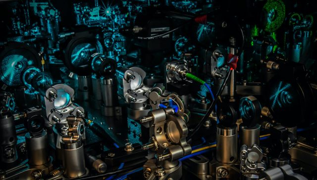
 Enlarge / Honeywell's ion trap hardware.
Over the years, academics developed a variety of systems that you could run quantum algorithms on. Most of these had one or two helpful traits—easy to manipulate or able to hold their state for longer—but lacked enough of the others to keep them from being practical computing solutions. Over the last few years, however, a number of companies have figured out how to manufacture significant numbers of solid-state qubits called transmons. Because the fabrication technology for transmons is similar to that of existing chipmaking, lots of the major players in the nascent market—including Google, IBM, and Rigetti—have settled on transmons.
But transmons aren't ideal either. They require extremely cold temperatures, show significant device-to-device variability, and are good but not great at holding their state. A number of people in the field I've talked to have suggested there's still room for another technology to surpass transmons, and Ars' own Chris Lee is putting his money on that happening.
Now, a company new to the quantum computing market is also betting it will. Honeywell, a company better known as a defense contractor and materials supplier, is announcing that it has built a quantum computer using an alternate technology called "ion trap" and will be making it available via Microsoft's Azure cloud service later this year. The company also claims that, by some measures, it's the most powerful quantum computer yet built, but that's a claim that needs to be considered very carefully.
Caught in a trap
Transmon qubits work by circulating current through a loop of superconducting wire, linked to a resonator that allows the state of the current to be controlled and readout. Both the superconducting wire and resonator, however, have to be manufactured, which allows for subtle differences between the individual qubits. In addition, all of that hardware has to be kept extremely cold—within a tiny fraction of a percent of absolute zero—in order to keep these relatively large objects near their quantum ground state.
Trapped ions provide a way around some of these challenges. The actual qubit is formed from a very small number of atoms—just two in Honeywell's case. Honeywell's president of Quantum Solutions, Tony Uttley, emphasized to Ars that this eliminates manufacturing issues, as every single device has identical properties defined by the atom being used (ytterbium in this case). "Every qubit starts perfect," Uttley told Ars. "Any error that you introduce is an error that you've put in place because of the surrounding infrastructure."
 Enlarge / Honeywell says its expertise in the support hardware led it to quantum computing. And, well, there's a lot of support hardware involved.
Honeywell
Because of Honeywell's experience with making and integrating this infrastructure, the company's engineers feel that they were in a great position to minimize this noise. The other thing is that small clusters of atoms like these can be cooled using lasers. While the environment has to be kept very cold, it doesn't have to reach the extreme temperatures needed by a transmon.
In Honeywell's case, the ytterbium ions weren't especially easy to cool using lasers, so they threw a couple of barium ions in the mix and cooled those with lasers. The ensemble of four ions was easy to cool and control, and the environment only had to be kept at 12K. This does require liquid helium but not the elaborate dilution refrigeration systems needed for Google and IBM's hardware.
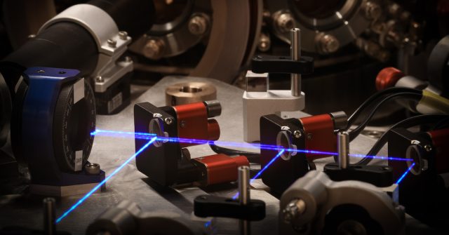
Because they're charged, the ions can be moved within the device simply by changing the local electric fields using the roughly 200 electrodes arranged along with the device. The state of the ion's electrons can be manipulated with lasers at specific wavelengths, which can put electrons in a superposition of potential energy states. Entanglement and various gate operations can be achieved simply by moving two ions into close proximity and by using laser operations that manipulate both simultaneously. The readout is achieved by stimulating the ions with yet another laser, which will cause the ions to emit a photon that's indicative of their state.
Honeywell’s device
Honeywell's hardware can be seen as a linear string of distinct devices. Ions enter at one end and are shuffled along through alternating regions where they can be held for storage or hit by lasers that perform qubit manipulation operations on them. A gate operation (the quantum equivalent of performing an AND or NOT operation) can be done by simply placing two ions in the same location and performing an operation on both of them simultaneously. In addition, clusters of four ions (two ytterbium, two barium) can be split in half, or two clusters of two ions can be merged.
The device Honeywell is describing today lines up four qubits along a single line of these storage/manipulation stages. But the diagram of the device also shows two additional lines of storage and manipulation stages flanking the line that was used in these initial experiments. This is in keeping with what Uttley told Ars: Honeywell is convinced the device can scale rapidly, with the expectation that additional qubits can be added each year without a fundamental change in architecture. So, while four qubits are quite low compared to what has been achieved with transmon devices (more on that in a bit), the company is expecting that it can narrow the gap very quickly.
 Enlarge / There is a LOT of lasers involved in controlling the states of these qubits.
One interesting aspect of this setup, which Uttley says isn't available on any other commercial system right now, is that you can measure a qubit individually without necessarily disturbing anything else in the system. (Technically, this is done by a science fiction-sounding operation called a quantum-teleportation CNOT gate.) This allows the computer to perform the equivalent of an "if" statement, changing the algorithm based on the results of measuring this single qubit. After the measurement, the qubit can also be reset and reused for further computation.
Individual components of this perform extremely well. One potential issue is what is called "state preparation and measurement errors," which have picked up the acronym SPAM. In this case, Honeywell's researchers find that the SPAM is dominated by measurement errors, but those occur less than 1 percent of the time. Single qubit gates have errors about an order of magnitude lower, and two-qubit gates are on a similar level. All of these are considerably lower than the typical behaviors of transmon gates.
Post a Comment